January 11, 2021 | By KJLC Innovate
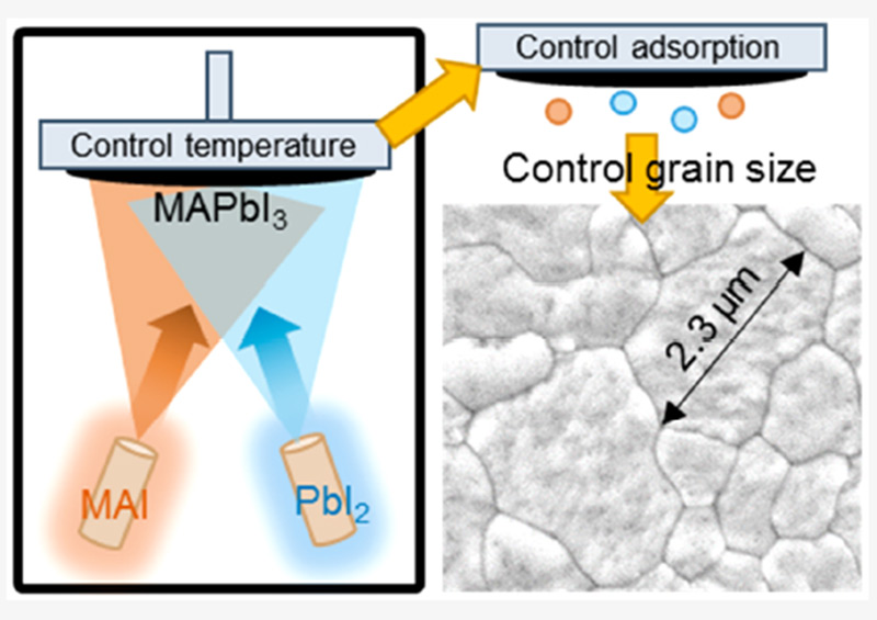
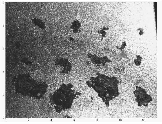
For nearly a decade the Kurt J Lesker Company has been shipping Physical Vapor Deposition (PVD) tools into the field of perovskite solar cells around the world and continues to support world class research into this exciting technology. A key topic in the fabrication of vapor deposited perovskite photovoltaics is how much the crystal grain boundaries affect the solar cell performance (see Figure 1). Recent work, published in ACS Energy Letters, titled "Control over crystal size in vapor deposited metal-halide perovskite films' by Killian Lohmann, Jay Patel, Mathias Uller Rothmann, Chelsea Xia, Robert Oliver, Laura Herz, Henry Snaith and Michael Johnston from the University of Oxford, in the UK, has not only identified key parameters that effect the grain growth in perovskite thin films but the team has also developed a novel method to control the deposition of the organic precursor, resulting in highly efficient solar cells.
Read More
Tags:
INNOVATE
Systems
Vacuum Science
Deposition Techniques
October 26, 2020 | By KJLC Innovate
The Kurt J. Lesker Company continues to support the researchers who are advancing the science and technology of spintronics around the world. Co2MnGa, a Heusler material, has been attractive to scientists as a novel magnetic conducting material on which spintronic structures like magnetic tunnel junctions can be built. Recent work, published in Applied Physics Letter titled "Perpendicular magnetic anisotropy in Co2MnGa and its anomalous Hall Effect" by Dr. Ludbrook, Dr. Ruck and Dr. Granville from Victoria University of Wellington, New Zealand, has identified characteristics of thin film Co2MnGa that are necessary for realizing magnetic tunnel junctions.
Read More
Tags:
INNOVATE
Systems
Vacuum Science
Deposition Techniques
October 01, 2020 | By KJLC Innovate

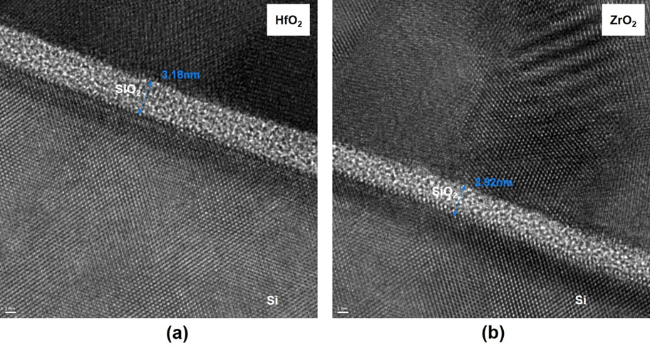
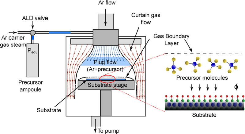
Dr. Zhigang Xiao, Professor of Electrical Engineering at Alabama A&M University, in collaboration with the ALD group in the Kurt J. Lesker Company recently developed the plasma-enhanced atomic layer deposition process and grow high dielectric constant (K) oxide for the application of electronic materials. They grew nanoscale hafnium dioxide (HfO2) and zirconium dioxide (ZrO2) thin films using remote plasma-enhanced atomic layer deposition (PE-ALD) and fabricated complementary metal-oxide semiconductor (CMOS) integrated circuits using the HfO2 and ZrO2 thin films as the gate oxide. Miniaturization in modern semiconductor industry requires thin film deposition to have atomic level control and the deposited film to be conformal and pinhole-free. As MOSFETs are scaled down to nanometer sizes, the tunneling currents through the gate dielectrics (the gate leakage current) has become a major concern in today’s fabrication of integrated circuits (ICs). High-K dielectric metal oxide could be a solution to the problem of the gate leakage current. The plasma-enhanced atomic layer deposition of HfO2 and ZrO2 thin films meets the requirement and can produce conformal and ultra-thin films with precise thickness control at the atomic layer level. The experimental results measured from the HfO2 and ZrO2 thin films were compared.
Read More
Tags:
INNOVATE
Systems
Vacuum Science
Deposition Techniques
June 16, 2020 | By KJLC Blog

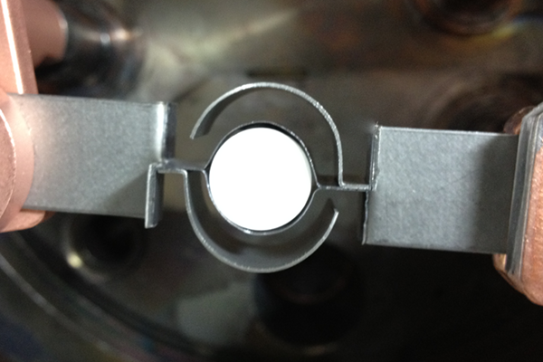
By far one of the most common questions that we receive from various users is how to thermally evaporate Aluminum. Aluminum is very commonly evaporated for various applications and can be somewhat problematic. Through some internal experience and through with working with various customers, we recommend two ways to approach thermal evaporation of aluminum.
Read More
Tags:
Vacuum Science
Deposition Materials
Deposition Techniques
June 01, 2020 | By KJLC Innovate

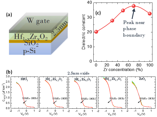
Dr. Kai Ni from the research group of Professor Suman Datta, Stinson Professor of Nanotechnology at the University of Notre Dame, in collaboration with Purdue University and Kurt J. Lesker Company recently developed conformal atomic layer deposition (ALD) based hafnium zirconium oxide thin film processes displaying excellent electrical properties for potential gate oxide complement or replacement in scaled logic and memory technology nodes. The findings were recently published and showcased in the IEEE International Electron Devices Meeting (IEDM) 2019 in San Francisco, CA [ref. 1]. In particular, hafnium zirconium oxide (HfxZr1-xO2, or HZO) has emerged as a ferroelectric (large charge density per unit area) material system that also displays a tunable permittivity or dielectric constant (charge response) depending on the concentration of Zr added to the base HfO2 oxide. The reported films indicate that by sweeping the concentration of Zr in HfO2 during the ALD growth, a substantial boost in the dielectric constant can be observed around 70% Zr concentration due to the presence of a crystallographic phase transition of the underlying HZO material structure, which results in enhanced electrical performance even in ultrathin films 25Å thick [ref. 2]. These findings elucidate the necessity and importance of extremely stringent deposition process control along with corresponding electrical and structural characterization for the understanding of new materials systems for their further implementation in commercial applications such as high-performance digital and analog CMOS technology at advanced nodes.
Read More
Tags:
INNOVATE
Systems
Vacuum Science
Deposition Techniques
May 01, 2020 | By KJLC Blog

In a recently issued patent (US 10,619,950 April 14, 2020) researchers at the Toyota Motor Company have demonstrated that the corrosion resistance of stainless steel exhaust systems for cars and trucks can be substantially improved by heat treatment in high vacuum. Stainless steel is a complex metal alloy of iron, nickel, chrome and other elements. It is known to be a very durable metal but even this robust material can be corroded by exposure to chloride ions, sulfuric and hydrochloric acids, soot and other artifacts of the exhaust from an internal combustion engine. Reaction with these aggressive gases causes pits in steel which eventually lead to premature failure. The use of low-grade fuels speeds the degradation of exhaust systems.
Read More
Tags:
INNOVATE
Systems
Vacuum Science
Deposition Techniques
April 21, 2020 | By KJLC Blog

As a Product Manager in the Materials Division, I field a lot of questions from customers from many different industries with varying degrees of sputtering experience. One of the more common emails that I receive goes something along the lines of, "There's something wrong with my bonding because the indium has melted out of the sides of my target." Often times the user has waited for their target, spent money on it, only to use it one time and had to stop due to the melted bond. A frustrating situation for sure.
Read More
Tags:
Vacuum Science
Deposition Materials
Deposition Techniques
March 06, 2020 | By KJLC Innovate

Dr. Nicholas A. Strnad (General Technical Services, LLC) in collaboration with the U.S. Army Combat Capabilities Command Army Research Laboratory and the University of Maryland, College Park have recently developed conformal processes for a variety of lead-based electronic materials with outstanding properties using atomic layer deposition (ALD)...
Read More
Tags:
INNOVATE
Systems
Vacuum Science
Deposition Techniques
July 22, 2019 | By KJLC Innovate

Sputtering is a relatively mature approach for the deposition of a variety of thin film materials. Initial publications on the process date to the early 1800s. In its simplest form sputtering provides a route to manufacture high quality reflective coatings for mirrors and potato chip bags; and at the extreme end, for creating the most advanced semiconductor computing devices in the world.
Read More
Tags:
INNOVATE
Systems
Vacuum Science
Deposition Techniques
May 09, 2018 | By KJLC Innovate

The current push to commercialize space travel has resulted in renewed demand to launch objects and even people into earth orbit or event deep space. Companies including SpaceX, Blue Origin and Rocket Lab have demonstrated the ability to make certain portions of a launch vehicle reusable and that may dramatically alter the cost to get to space. True rocket ship factories are emerging which, in one case, can put out a couple of full blown launch vehicles every month!
Read More
Tags:
INNOVATE
Systems
Vacuum Science
Deposition Techniques
Previous Entries
Next Entries
